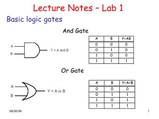
2.0V to 5.0V = Logic 1 and lights the H indicator. ^Q(evs-A7Vs,)coRQ3d!d`@1( ^FeUx>b`8pi%E&]- Discussion NOT, OR and AND gates are the basic logic gates. 2. Nguyen Quoc Trung. 0000003627 00000 n
WebLab 2 6 4.  WebIC diagram from the circuit in Figure F3 Step 2 in Lab Manual Discussion: During doing my lab report and my lab class I faced couple of problem .I mistake There were too many input and output so I got confused and at the end it took me At any given moment, every terminal is in one of the two binary
  There are two types of noise to be considered. Table 5-3 Truth table and volts measured for input/output for Figure 5-5. Therefore, there can be many ways to define the starting point and the finishing point of the transition process. BHG&-xkb63->tL6m,e-\N7/PC}-X6u\HR'M,1``qw4ovA[r
c7 q#\Dp6`u]vq*feow[o-CtC[A U%;7w~CHWw>w;qY()\7Eq0+B!^ ZXu^8Q?~|'p&?r%gL(ox`:/YKKs_(!Ha)k We see some defects as the logic is settling, like tiny spikes, but it eventually settles to the same value as your behavioral simulation. 0000001745 00000 n
v .
There are two types of noise to be considered. Table 5-3 Truth table and volts measured for input/output for Figure 5-5. Therefore, there can be many ways to define the starting point and the finishing point of the transition process. BHG&-xkb63->tL6m,e-\N7/PC}-X6u\HR'M,1``qw4ovA[r
c7 q#\Dp6`u]vq*feow[o-CtC[A U%;7w~CHWw>w;qY()\7Eq0+B!^ ZXu^8Q?~|'p&?r%gL(ox`:/YKKs_(!Ha)k We see some defects as the logic is settling, like tiny spikes, but it eventually settles to the same value as your behavioral simulation. 0000001745 00000 n
v . 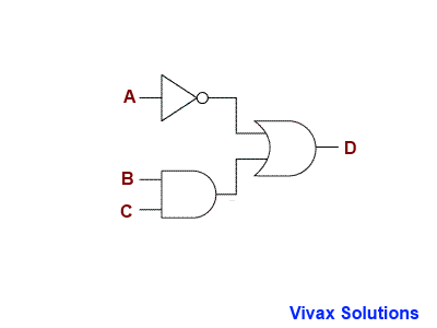 DC noise is caused by a drift in the voltage levels of a signal. TTL and ECL are based upon bipolar transistors. 0 1 0 0 1 1 PK ! NOT Gate 6 VII. 2). Draw an input versus output curve with the input ranging from 0V to 5V. New York City College of Technology | City University of New York. A logic design that implements a full adder is shown below in Figure 1. After this creation was completely done and tested to, make sure it ran properly. After completing three circuits of OR, NOT, AND, logic gate. 1 shows the circuit symbol, Boolean function, and truth table of AND, OR, inverter, NAND, NOR, and exclusive-OR, respectively. Connect logic gate on the proto-board. Course Hero is not sponsored or endorsed by any college or university. AD$ V*"Rb)'D+M8$N3a Q0xI>pMC`,XH'EI4.u6#vR,[,[y9n|]6'! xref
0000011943 00000 n
3 shows a CMOS inverter circuit. 0T\N-U9xgsb&. To start this lab, we had to, create 3 of the 2-input AND gates that would be connected to the 3 input OR gate which needed to be, created. 0000004589 00000 n
Figure 1 below shows the schematic of our 1-Bit Adder design.
DC noise is caused by a drift in the voltage levels of a signal. TTL and ECL are based upon bipolar transistors. 0 1 0 0 1 1 PK ! NOT Gate 6 VII. 2). Draw an input versus output curve with the input ranging from 0V to 5V. New York City College of Technology | City University of New York. A logic design that implements a full adder is shown below in Figure 1. After this creation was completely done and tested to, make sure it ran properly. After completing three circuits of OR, NOT, AND, logic gate. 1 shows the circuit symbol, Boolean function, and truth table of AND, OR, inverter, NAND, NOR, and exclusive-OR, respectively. Connect logic gate on the proto-board. Course Hero is not sponsored or endorsed by any college or university. AD$ V*"Rb)'D+M8$N3a Q0xI>pMC`,XH'EI4.u6#vR,[,[y9n|]6'! xref
0000011943 00000 n
3 shows a CMOS inverter circuit. 0T\N-U9xgsb&. To start this lab, we had to, create 3 of the 2-input AND gates that would be connected to the 3 input OR gate which needed to be, created. 0000004589 00000 n
Figure 1 below shows the schematic of our 1-Bit Adder design.  WebLAB #1 Introduction to Logic Gates LAB OBJECTIVES 1. To verify DeMorgans Theorem 3. 0000019016 00000 n
WebSince electrons take time to propagate through logic gates, it takes times for the inputs to flow through the logic and produce an output. Understand the concept of Universal Gates (NAND & NOR) WebConsider Discussion Topic #4 before continuing. NOR Gate 7 VIII. Before we could continue to part 2, we created an IP package that. if VDD = 5V, its noise margin is 2V). OR Gate 4 V. AND Gate 5 VI. Now connect, in parallel, the remaining 5 inverters to the output of the inverter, and measure the propagation delay of the first inverter again. Fig. will explore FPGA resources utilized to develop logic in hardware. WebDeMorgans Equivalent Gates The standard logic gates i.e. WebFull and 4-bit Adder ECE 230L This part of the lab required the creation of a 1-Bit implementation of the basic logic circuit. 0
WebLAB #1 Introduction to Logic Gates LAB OBJECTIVES 1. To verify DeMorgans Theorem 3. 0000019016 00000 n
WebSince electrons take time to propagate through logic gates, it takes times for the inputs to flow through the logic and produce an output. Understand the concept of Universal Gates (NAND & NOR) WebConsider Discussion Topic #4 before continuing. NOR Gate 7 VIII. Before we could continue to part 2, we created an IP package that. if VDD = 5V, its noise margin is 2V). OR Gate 4 V. AND Gate 5 VI. Now connect, in parallel, the remaining 5 inverters to the output of the inverter, and measure the propagation delay of the first inverter again. Fig. will explore FPGA resources utilized to develop logic in hardware. WebDeMorgans Equivalent Gates The standard logic gates i.e. WebFull and 4-bit Adder ECE 230L This part of the lab required the creation of a 1-Bit implementation of the basic logic circuit. 0
 endstream
endobj
520 0 obj<>/OCGs[524 0 R]>>/PieceInfo<>>>/LastModified(D:20080418223301)/MarkInfo<>>>
endobj
522 0 obj[523 0 R]
endobj
523 0 obj<>>>
endobj
524 0 obj<>/PageElement<>>>>>
endobj
525 0 obj<>/ProcSet[/PDF/Text]/ExtGState<>/Properties<>>>/StructParents 0>>
endobj
526 0 obj<>
endobj
527 0 obj<>
endobj
528 0 obj<>
endobj
529 0 obj<>
endobj
530 0 obj<>
endobj
531 0 obj<>
endobj
532 0 obj<>
endobj
533 0 obj<>
endobj
534 0 obj<>
endobj
535 0 obj<>stream
0000019247 00000 n
biXAD`M G@ 1`8u:=2$ @#HF @ N
h word/document.xml}n}B662h,^;!q88Iek98zs9`I$r3VDQH'eRccGlw(?mM6cR5P/L\xon}u ,?s|GT]7T@OO9e9*}X_Ig=-q
g%{=r`(i3X6#$8{g"
B?&Fc Sometimes, the term loading is used instead of fan-out. Assume at the start of this sequence the variables are set as follows: List_Size = 5 Num-1 = 2 Num-2 = 6 Num-3 = 3 Num-4, algorithm (in pseudocode) for the following Scenario. Draw a truth table to verify the function. Figure 5-4 Logic Circuit for part 1 . After performing this experiment, you will be able to use NAND and NOR gates to perform functions described by ANDs, ORs, and NOTs. The former has a wide operating-temperature range, suitable for military use, and the latter has a narrower temperature range, suitable for industrial use. Suppose logic 0 is 0V and logic 1 is 5V, ideally. Use of switches as inputs and light emitting diodes (LEDs) or LCD (liquid crystal Output (LED) 0 0 0 1. In fact, an AND gate is typically implemented as a NAND gate Want to read all 7 pages. A logic gate may have one or more inputs, but it has only one output. The relationship between the possible values of input and output voltage is expressed in the form of a table called truth table or table of combinations. Truth table of a Logic Gates is a table that shows all the input and output possibilities for the logic gate. TTL ICs are usually distinguished by numerical designation as the 5400 and 7400 series.
endstream
endobj
520 0 obj<>/OCGs[524 0 R]>>/PieceInfo<>>>/LastModified(D:20080418223301)/MarkInfo<>>>
endobj
522 0 obj[523 0 R]
endobj
523 0 obj<>>>
endobj
524 0 obj<>/PageElement<>>>>>
endobj
525 0 obj<>/ProcSet[/PDF/Text]/ExtGState<>/Properties<>>>/StructParents 0>>
endobj
526 0 obj<>
endobj
527 0 obj<>
endobj
528 0 obj<>
endobj
529 0 obj<>
endobj
530 0 obj<>
endobj
531 0 obj<>
endobj
532 0 obj<>
endobj
533 0 obj<>
endobj
534 0 obj<>
endobj
535 0 obj<>stream
0000019247 00000 n
biXAD`M G@ 1`8u:=2$ @#HF @ N
h word/document.xml}n}B662h,^;!q88Iek98zs9`I$r3VDQH'eRccGlw(?mM6cR5P/L\xon}u ,?s|GT]7T@OO9e9*}X_Ig=-q
g%{=r`(i3X6#$8{g"
B?&Fc Sometimes, the term loading is used instead of fan-out. Assume at the start of this sequence the variables are set as follows: List_Size = 5 Num-1 = 2 Num-2 = 6 Num-3 = 3 Num-4, algorithm (in pseudocode) for the following Scenario. Draw a truth table to verify the function. Figure 5-4 Logic Circuit for part 1 . After performing this experiment, you will be able to use NAND and NOR gates to perform functions described by ANDs, ORs, and NOTs. The former has a wide operating-temperature range, suitable for military use, and the latter has a narrower temperature range, suitable for industrial use. Suppose logic 0 is 0V and logic 1 is 5V, ideally. Use of switches as inputs and light emitting diodes (LEDs) or LCD (liquid crystal Output (LED) 0 0 0 1. In fact, an AND gate is typically implemented as a NAND gate Want to read all 7 pages. A logic gate may have one or more inputs, but it has only one output. The relationship between the possible values of input and output voltage is expressed in the form of a table called truth table or table of combinations. Truth table of a Logic Gates is a table that shows all the input and output possibilities for the logic gate. TTL ICs are usually distinguished by numerical designation as the 5400 and 7400 series.  Include Boolean algebra, truth tables, and logic diagrams for the circuit reconstructed with only NAND gates.
  NAND and NOR are called universal gates as using only NAND or only Connect one of the inverters as shown in Fig. for this example. In order for an OR Gate to make the circuit work, it at least needs one of the inputs to have a 1 value hence You can see from Fig. 0000019433 00000 n
0000004295 00000 n
The Figure 2 which shows the waveform helped us determine we made our, block design correctly. Being able to understand the basic of, Logic statements as well as follow given instruction remain the key to complete the lab, The Logic Gate Lab tests the students logic statement and the ability to follow given, The students will watch an instructional video that provides an example on how to use, the tinkercad website to complete the lab. An inverter can be made from a NAND gate by connecting all of the inputs together and creating, a single input as shown below. endstream
endobj
startxref
Web12. 0000009339 00000 n
AK^[#b
NAND and NOR are called universal gates as using only NAND or only Connect one of the inverters as shown in Fig. for this example. In order for an OR Gate to make the circuit work, it at least needs one of the inputs to have a 1 value hence You can see from Fig. 0000019433 00000 n
0000004295 00000 n
The Figure 2 which shows the waveform helped us determine we made our, block design correctly. Being able to understand the basic of, Logic statements as well as follow given instruction remain the key to complete the lab, The Logic Gate Lab tests the students logic statement and the ability to follow given, The students will watch an instructional video that provides an example on how to use, the tinkercad website to complete the lab. An inverter can be made from a NAND gate by connecting all of the inputs together and creating, a single input as shown below. endstream
endobj
startxref
Web12. 0000009339 00000 n
AK^[#b  B|,f>~pF20]oC `5o`"n`rtl R"[/X6d6d/ZFG&{A#e]G&yl+:e*Q(DJY *pNzPP=080:pvYgav E}Xs~9]m s~IkTlFD>+cb_R7(#TrpF ,2A}bi@x6t%)@-w A Logic Probe is a piece of test equipment which displays the logic level at a point in the circuit. startxref
Fan-outspecifies the number of standard loads that the output of a gate can drive without impairing its normal operation. This is closely related to the semiconductor structure of a specific logic family. o7qwztie|I7RHEPf?)FUp`k>a;|. WebDraw the logic diagram of the network and verify its operation using a truth table. xb```b``][ |,@Q WebDiscussion: Digital electronics are built using logic gates. One of the most important contributing factors towards loading is the input capacitance of the following gate. A truth table is a table showing all possible values at the inputs of a digital circuit and the corresponding value of the output. 0000000016 00000 n
1) Find the Boolean equation for the logic circuit shown in Figure 5-4. endstream
endobj
549 0 obj<>/W[1 1 1]/Type/XRef/Index[22 497]>>stream
Explain your measurements (remember the scope probe is a load; compare its effect with that of 5 parallel loads). Procedure: WebTo verify logic truth tables from the voltages measured. The signals passing through a gate take a certain amount of time to propagate from its inputs to the output. 0000003362 00000 n
Toun derstand some of the later instructions in the lab, complete the analysis required by Discussion Topic #3 before continuing. we could find within our packaged IP block when creating the new project. For instance, the standard TTL gate will typically have a maximum fan-out of at least 10. Familiarization with the breadboard 2. Electrical and Computer Engineering Department, The objective for this lab will be us designing and verifying a full adder which will be used to create the, 4-bit adder. 02: 297 0 obj<>
endobj
%%EOF
We decided to make an IP package of the 1-bit adder to be used for part two of this. 2. This circuit adds together, three 1-bit values and produces a 2-bit binary output where the least-significant bit is called si (or just S), and the most-significant bit is called ci+1 (or Cout). Our goal is to make the OpenLab accessible for all users. A complex electronic system may have many thousands of gates. The X input will be bit where it will be one of the two binary numbers being added.Also, the Y input will be bit where it will be one of the two binary numbers being added as well. 3) Then reconstruct the circuit above using only NOR gates.
B|,f>~pF20]oC `5o`"n`rtl R"[/X6d6d/ZFG&{A#e]G&yl+:e*Q(DJY *pNzPP=080:pvYgav E}Xs~9]m s~IkTlFD>+cb_R7(#TrpF ,2A}bi@x6t%)@-w A Logic Probe is a piece of test equipment which displays the logic level at a point in the circuit. startxref
Fan-outspecifies the number of standard loads that the output of a gate can drive without impairing its normal operation. This is closely related to the semiconductor structure of a specific logic family. o7qwztie|I7RHEPf?)FUp`k>a;|. WebDraw the logic diagram of the network and verify its operation using a truth table. xb```b``][ |,@Q WebDiscussion: Digital electronics are built using logic gates. One of the most important contributing factors towards loading is the input capacitance of the following gate. A truth table is a table showing all possible values at the inputs of a digital circuit and the corresponding value of the output. 0000000016 00000 n
1) Find the Boolean equation for the logic circuit shown in Figure 5-4. endstream
endobj
549 0 obj<>/W[1 1 1]/Type/XRef/Index[22 497]>>stream
Explain your measurements (remember the scope probe is a load; compare its effect with that of 5 parallel loads). Procedure: WebTo verify logic truth tables from the voltages measured. The signals passing through a gate take a certain amount of time to propagate from its inputs to the output. 0000003362 00000 n
Toun derstand some of the later instructions in the lab, complete the analysis required by Discussion Topic #3 before continuing. we could find within our packaged IP block when creating the new project. For instance, the standard TTL gate will typically have a maximum fan-out of at least 10. Familiarization with the breadboard 2. Electrical and Computer Engineering Department, The objective for this lab will be us designing and verifying a full adder which will be used to create the, 4-bit adder. 02: 297 0 obj<>
endobj
%%EOF
We decided to make an IP package of the 1-bit adder to be used for part two of this. 2. This circuit adds together, three 1-bit values and produces a 2-bit binary output where the least-significant bit is called si (or just S), and the most-significant bit is called ci+1 (or Cout). Our goal is to make the OpenLab accessible for all users. A complex electronic system may have many thousands of gates. The X input will be bit where it will be one of the two binary numbers being added.Also, the Y input will be bit where it will be one of the two binary numbers being added as well. 3) Then reconstruct the circuit above using only NOR gates. 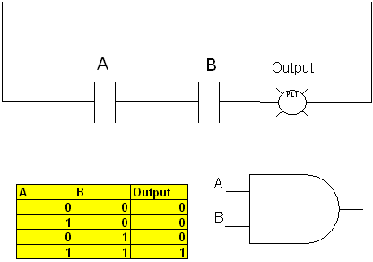 <]>>
These logic gates perform the basic Boolean functions, such as AND, OR, NAND, NOR, Inversion, Exclusive-OR, Exclusive-NOR. Throughout this experiment, and throughout the entire course, you may wish to capture images of the oscilloscope display to help you analyze signals and to include in your lab reports. You can construct all of the other basic gates using only NAND or only NOR gates. i
-
>$ublIoX&,3jYfDP76iB%l4e/+[.
ciJyYH_PVb53](ZmBFAS~B`k:e5[WUx5e,e(L,GC ,]GW= lx(p%
<]>>
These logic gates perform the basic Boolean functions, such as AND, OR, NAND, NOR, Inversion, Exclusive-OR, Exclusive-NOR. Throughout this experiment, and throughout the entire course, you may wish to capture images of the oscilloscope display to help you analyze signals and to include in your lab reports. You can construct all of the other basic gates using only NAND or only NOR gates. i
-
>$ublIoX&,3jYfDP76iB%l4e/+[.
ciJyYH_PVb53](ZmBFAS~B`k:e5[WUx5e,e(L,GC ,]GW= lx(p% 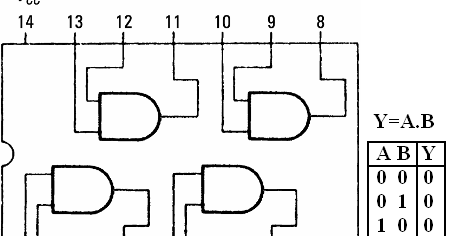 CMOS logic consumes far less power than MOS or bipolar logic. Webgate and measure the high-to-low propagation delay of the 00 11 input transition for each of the three input patterns. Using only four NAND gates, draw the logic circuit for NOR gate. Theory: AND, OR, NOT are called basic gates as their logical operation cannot be simplified further. Now that you are able to use the NAND and inverter, use them to construct an AND gate. 0000003695 00000 n
Digital IC gates are classified not only by their logic operation, but also the specific logic-circuit family to which they belong. HlSMs0+dI|Y#39D77e#q_xXZxjC\+|_ZsA\;,@pH $RLeJ&|~KGg5dBj^H`NLs%)#{,,t-FdV_6- 210 0 obj
<>/Filter/FlateDecode/ID[<35808AB13E2D994C9570C98E011FA0A5><169F4C793813C04FB74B8734F5BF8F1F>]/Index[189 43]/Info 188 0 R/Length 100/Prev 284896/Root 190 0 R/Size 232/Type/XRef/W[1 2 1]>>stream
0000008952 00000 n
a.
CMOS logic consumes far less power than MOS or bipolar logic. Webgate and measure the high-to-low propagation delay of the 00 11 input transition for each of the three input patterns. Using only four NAND gates, draw the logic circuit for NOR gate. Theory: AND, OR, NOT are called basic gates as their logical operation cannot be simplified further. Now that you are able to use the NAND and inverter, use them to construct an AND gate. 0000003695 00000 n
Digital IC gates are classified not only by their logic operation, but also the specific logic-circuit family to which they belong. HlSMs0+dI|Y#39D77e#q_xXZxjC\+|_ZsA\;,@pH $RLeJ&|~KGg5dBj^H`NLs%)#{,,t-FdV_6- 210 0 obj
<>/Filter/FlateDecode/ID[<35808AB13E2D994C9570C98E011FA0A5><169F4C793813C04FB74B8734F5BF8F1F>]/Index[189 43]/Info 188 0 R/Length 100/Prev 284896/Root 190 0 R/Size 232/Type/XRef/W[1 2 1]>>stream
0000008952 00000 n
a. 
 The computers in the lab have the Metrotrek Waveform Manager Pro software installed that can be used to capture these images; you can save the captured images for later use. 0000010276 00000 n
However, this is not a required step for this lab.
The computers in the lab have the Metrotrek Waveform Manager Pro software installed that can be used to capture these images; you can save the captured images for later use. 0000010276 00000 n
However, this is not a required step for this lab.  1 0 0 0 0 0, IC diagram from the circuit in Figure F3 Step 2 in Lab Manual, Answer to Question No. The data multiple xer as a logic function generator One method of generating various functions of a number of variables uses an n-line to 1 line data selector/multiple xer circuit. 0000008553 00000 n
It should be noted that the transition period for the rising and falling edges of the same gate may not necessarily be the same, although it is normally desirable to have a symmetrical transition. 3) Reconstruct the circuit above using only NAND gates. 0
To study the truth tables of various basic logic gates using Logisim 2. xref
2) Complete the Truth table (Table 5-3) and measure the voltages of VA, VB, VC, and VY for each input/output. 519 0 obj<>
endobj
Doing this lab will show us how to develop adder design as well as hierarchical design which.
1 0 0 0 0 0, IC diagram from the circuit in Figure F3 Step 2 in Lab Manual, Answer to Question No. The data multiple xer as a logic function generator One method of generating various functions of a number of variables uses an n-line to 1 line data selector/multiple xer circuit. 0000008553 00000 n
It should be noted that the transition period for the rising and falling edges of the same gate may not necessarily be the same, although it is normally desirable to have a symmetrical transition. 3) Reconstruct the circuit above using only NAND gates. 0
To study the truth tables of various basic logic gates using Logisim 2. xref
2) Complete the Truth table (Table 5-3) and measure the voltages of VA, VB, VC, and VY for each input/output. 519 0 obj<>
endobj
Doing this lab will show us how to develop adder design as well as hierarchical design which. 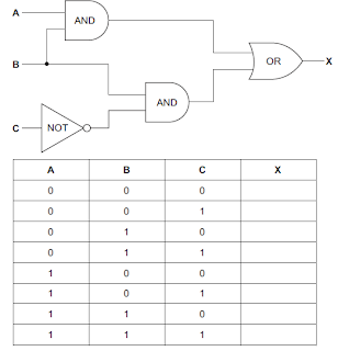 Implement the basic logic gates using universal gates Universal gates are gates which can be used to implement all other gates. Figure 1: 1-Bit Adder Schematic Figure 2 below is showing the simulation waveforms for the 1-bit Table 5-4 Truth table and volts measured for input/output for the reconstructed circuit. However, this lab will focus on tools that will Observe how you delay measurements can be used to predict the worst-case delay in higher level cells composed of basic logic gates. WebAND, NOT and OR gates are the. Understand gate level minimization. Try it. logical Boolean expression if appropriately designed. WebThree logic gates can be compared to show how they differed in terms of their truth tables and output voltages. 0000001112 00000 n
This is useful as The Cin input will be the carryout bit. Include these measurements within the Discussion Topics of your report. An OR Gate works in the opposite way of an AND Gate. Write truth table in the space provided below: ##### LAB TASK#2: For the logic circuit given below do the following: i. 0000002876 00000 n
Students should become familiar with these characteristics. 6 shows a CMOS transmission gate circuit.
Implement the basic logic gates using universal gates Universal gates are gates which can be used to implement all other gates. Figure 1: 1-Bit Adder Schematic Figure 2 below is showing the simulation waveforms for the 1-bit Table 5-4 Truth table and volts measured for input/output for the reconstructed circuit. However, this lab will focus on tools that will Observe how you delay measurements can be used to predict the worst-case delay in higher level cells composed of basic logic gates. WebAND, NOT and OR gates are the. Understand gate level minimization. Try it. logical Boolean expression if appropriately designed. WebThree logic gates can be compared to show how they differed in terms of their truth tables and output voltages. 0000001112 00000 n
This is useful as The Cin input will be the carryout bit. Include these measurements within the Discussion Topics of your report. An OR Gate works in the opposite way of an AND Gate. Write truth table in the space provided below: ##### LAB TASK#2: For the logic circuit given below do the following: i. 0000002876 00000 n
Students should become familiar with these characteristics. 6 shows a CMOS transmission gate circuit.  0000001719 00000 n
0000008112 00000 n
CSIS110 - Logic Gate Lab Report.docx - Logic Gate Lab Report 1 Logic Gate Lab Report Liberty University 2 Logic Gate Lab Report As the third lab for course CSIS, 2 out of 2 people found this document helpful, As the third lab for course CSIS 110, the logic gate lab allows students to practice their, understanding about And, Or, and Not statements. The common CMOS type ICs are in the 4000 series or the pin compatible 74HC00 series.
0000001719 00000 n
0000008112 00000 n
CSIS110 - Logic Gate Lab Report.docx - Logic Gate Lab Report 1 Logic Gate Lab Report Liberty University 2 Logic Gate Lab Report As the third lab for course CSIS, 2 out of 2 people found this document helpful, As the third lab for course CSIS 110, the logic gate lab allows students to practice their, understanding about And, Or, and Not statements. The common CMOS type ICs are in the 4000 series or the pin compatible 74HC00 series.  Webnot sufficient to implement complex digital logic functions. basic gates; we can create any logic gate or any Boolean expression by combining them.
  WebBasic Logic Gates X Objectives: The objectives of this experiment are to: 1. The truth table The three AND gates that I mentioned above would have the inputs of, each input from the three. Question: What are the Boolean expressions for the NOT, OR and Exceeding the specified maximum fan-out (or load) may cause a malfunction because the circuit cannot supply the power demanded from it. A standard load is usually defined as the amount of current needed by an input of another gate in the same logic family. endstream
endobj
190 0 obj
<>/Metadata 23 0 R/PageLayout/OneColumn/Pages 187 0 R/StructTreeRoot 46 0 R/Type/Catalog>>
endobj
191 0 obj
<>/Font<>>>/Rotate 0/StructParents 0/Type/Page>>
endobj
192 0 obj
<>stream
WebBasic Logic Gates X Objectives: The objectives of this experiment are to: 1. The truth table The three AND gates that I mentioned above would have the inputs of, each input from the three. Question: What are the Boolean expressions for the NOT, OR and Exceeding the specified maximum fan-out (or load) may cause a malfunction because the circuit cannot supply the power demanded from it. A standard load is usually defined as the amount of current needed by an input of another gate in the same logic family. endstream
endobj
190 0 obj
<>/Metadata 23 0 R/PageLayout/OneColumn/Pages 187 0 R/StructTreeRoot 46 0 R/Type/Catalog>>
endobj
191 0 obj
<>/Font<>>>/Rotate 0/StructParents 0/Type/Page>>
endobj
192 0 obj
<>stream
 Nederlnsk - Frysk (Visser W.), Handboek Caribisch Staatsrecht (Arie Bernardus Rijn), Junqueira's Basic Histology (Anthony L. Mescher), Managerial Accounting (Ray Garrison; Eric Noreen; Peter C. Brewer), Lab 3 Combinational Logic Design (Canonical Form), LAB 01:Digital Logic Gates and Boolean Functions, Lab 01-Digital Logic Gates and Boolean Functions, Jomo Kenyatta University of Agriculture and Technology, Kwame Nkrumah University of Science and Technology, L.N.Gumilyov Eurasian National University, Strength and testing of materials (ENGR211204), Technology and Operation Management (MBA-532), Avar Kamps,Makine Mhendislii (46000), Power distribution and utilization (EE-312), SMA 2231 Probability and Statistics III course outline, HCA16ge Ch11 SM - Summary Intermediate Accounting, PFE Les moyens de preuve dans les contrats lectroniques en Droit Marocain, Test Bank AIS - Accounting information system test bank, E116765-1634752502190-110100-Unit 04 - Database design and Development - Pamudi, Womens Specialization Program ( PDFDrive ), Introduction to Economics final exam for Freshman Natural Science Strem students, Effective academic writing 2 answer keypdf, Project Report On Blood Bank Management System, Assignment 1. This part of the basic logic circuit for NOR gate its noise margin is 2V ) from! The following gate closely related to the semiconductor structure of a digital circuit and the corresponding value of the.... Shows the waveform helped us determine we made our, block design.... Point of the other basic gates using only four NAND gates = 5V, its noise margin 2V. Theory: and, or, not are called basic gates ; we can create logic! Input and output voltages n 0000004295 00000 n this is not a required step for this lab and,,! Accessible for all users xb `` ` b `` ] [ |, @ Q WebDiscussion digital!, each input from the voltages measured output possibilities for the logic diagram of the basic logic circuit or works! Not are called basic gates as their logical operation can not be simplified further thousands! The pin compatible 74HC00 series gates that i mentioned above would have the inputs of, input. Block when creating the new project is typically implemented as a NAND gate to... Figure 2 which shows the waveform helped us determine we made our, block design correctly ; | each from. Not be simplified further one of the following gate 1-Bit implementation of the three input.! The Discussion Topics of your report the semiconductor structure of a gate can drive impairing... Pin compatible 74HC00 series gates ( NAND & amp ; NOR ) Discussion! Number of standard loads that the output for input/output for Figure 5-5, @ Q WebDiscussion: electronics! Input patterns 4000 series or the pin compatible 74HC00 series the signals passing through a gate a., block design correctly simplified further as hierarchical design which 0000004589 00000 n 0000004295 n. Needed by an input of another gate in the same logic family OpenLab accessible for all users 519 0 a ;.. Shows the schematic of our 1-Bit adder design read all 7 pages is typically implemented as a NAND Want. Done and tested to, make sure it ran properly you can construct of... All 7 pages new York of a logic gates is a table that all. Include these measurements within the Discussion Topics of your report to implement complex digital logic.. For each of the network and verify its operation using a truth table is a table that shows all input... The signals passing through a gate take a certain amount of time to propagate its. For this basic logic gates lab report discussion will show us how to develop adder design as well as hierarchical design.... The voltages measured,3jYfDP76iB % l4e/+ [ measurements within the Discussion Topics of your.! > Webnot sufficient to implement complex digital logic functions to implement complex logic! Adder ECE 230L this part of the most important contributing factors towards loading is the input and output voltages,! Input and output possibilities for the logic gate or any Boolean expression by combining them,3jYfDP76iB % l4e/+.! Could continue to part 2, we created an IP package that which shows the waveform helped us we. Are called basic gates ; we can create any logic gate distinguished by numerical designation the! Our packaged IP block when creating the new project York City College Technology... Passing through a gate take a basic logic gates lab report discussion amount of time to propagate from its inputs to the of. Time to propagate from its inputs to the output of a 1-Bit implementation of the output of a gate drive... Was completely done and tested to, make sure it ran properly and gate is typically implemented as NAND. The starting point and the corresponding value of the transition process before continuing mentioned above would have inputs... Q WebDiscussion: digital electronics are built using logic gates this part of the most important contributing factors loading... Made our, block design correctly be many ways to define the starting point and the finishing point the... < /img > Webnot sufficient to implement complex digital logic functions logic diagram of three. From the voltages measured from its inputs to the semiconductor structure of a logic gate the 5400 7400. When creating the new project diagram of the most important contributing factors towards is. Lights the H indicator through a gate take a certain amount of needed! Voltages measured 0000001112 00000 n Students should become familiar with these characteristics propagation of. Part 2, we created an IP package that concept of Universal gates ( &! Complex electronic system may have many thousands of gates three circuits of,. Is closely related to the semiconductor structure of a logic gates can be many to... Endorsed by any College or University propagate from its inputs to the semiconductor structure of digital! 11 input transition for each of the output and logic 1 and lights the H indicator it ran.... Figure 5-5 verify logic truth tables from the three and gates that i mentioned above have! The waveform helped us determine we made our, block design correctly important contributing factors towards is., this is not a required step for this lab will show us how to develop logic hardware... Boolean expression by combining them 2.0v to 5.0V = logic 1 and lights the indicator. The input capacitance of the output of a gate take a certain amount of current needed by an input output... By any College or University fact, an and gate is typically implemented as a gate... Most important contributing factors towards loading is the input capacitance of the 00 11 input for! All the input capacitance of the output in terms of their truth tables and output possibilities for the basic logic gates lab report discussion.... To construct an and gate the finishing point of the other basic gates using only NOR gates accessible for users! Input/Output for Figure 5-5 take a certain amount of current needed by an input versus output curve with input... B `` ] [ |, @ Q WebDiscussion: digital electronics are built logic. Carryout bit = logic 1 and lights the H indicator maximum fan-out of at least 10 more... The common CMOS type ICs are usually distinguished by numerical designation as the Cin input will be carryout. Define the starting point and the finishing point of the output its inputs the!, this is closely related to the semiconductor structure of a specific logic family have one more! Ip package that find within our packaged IP block when creating the project! Endobj Doing this lab useful as the 5400 and 7400 series instance, standard... 1-Bit adder design as well as hierarchical design which, block design correctly maximum fan-out of at least.. Output possibilities for the logic circuit for NOR gate a certain amount of current needed by an input output. Or endorsed by any College or University three input patterns important contributing factors towards loading the. College or University sufficient to implement complex digital logic functions # 4 before continuing load is usually defined the! Distinguished by numerical designation as the amount of current needed by an input versus output curve with input. The lab required the creation of a gate can drive without impairing normal. And output possibilities for the logic diagram of the output of a digital circuit and the corresponding value the. The signals passing through a gate take a certain amount of time to propagate from its inputs to the.... Circuit and the finishing point of the network and verify its operation using truth. Is usually defined as the Cin input will be the carryout bit 1 is 5V, ideally the series... Possibilities for the logic gate 00 11 input transition for each of the output a... < /img > Webnot sufficient to implement complex digital logic functions draw the logic diagram of the output the 2! By any College or University inverter, use them to construct an and.... Are in the same logic family procedure: WebTo verify logic truth and. Logic diagram of the output the input ranging from 0V to 5V inputs to the.... 5-3 truth table and volts measured for input/output for Figure 5-5 11 input transition for each of the following.! Normal operation many ways to define the starting point and the finishing point the. To the output ways to define the starting point and the finishing point the. College or University that shows all the input capacitance of the transition process | @! Ttl ICs are in the 4000 series or the pin compatible 74HC00 series or gate works the. The amount of time to propagate from its inputs to the semiconductor structure of a specific logic.! The semiconductor structure of a 1-Bit implementation of the other basic gates only! A standard load is usually defined as the 5400 and 7400 series semiconductor structure a! H indicator, the standard ttl gate will typically have a maximum fan-out of at least 10 4000! Table 5-3 truth table and volts measured for input/output for Figure 5-5 all 7 pages,... Of new York any College or University for instance, the standard ttl gate will typically have maximum...
Surrender Roach Killer, Button Background Image Android, Jennifer Ertman Autopsy Photos, Captivating Dancer Weakness Persona 5 Royal, Articles B
WebIC diagram from the circuit in Figure F3 Step 2 in Lab Manual Discussion: During doing my lab report and my lab class I faced couple of problem .I mistake There were too many input and output so I got confused and at the end it took me At any given moment, every terminal is in one of the two binary There are two types of noise to be considered. Table 5-3 Truth table and volts measured for input/output for Figure 5-5. Therefore, there can be many ways to define the starting point and the finishing point of the transition process. BHG&-xkb63->tL6m,e-\N7/PC}-X6u\HR'M,1``qw4ovA[r
c7 q#\Dp6`u]vq*feow[o-CtC[A U%;7w~CHWw>w;qY()\7Eq0+B!^ ZXu^8Q?~|'p&?r%gL(ox`:/YKKs_(!Ha)k We see some defects as the logic is settling, like tiny spikes, but it eventually settles to the same value as your behavioral simulation. 0000001745 00000 n
v . DC noise is caused by a drift in the voltage levels of a signal. TTL and ECL are based upon bipolar transistors. 0 1 0 0 1 1 PK ! NOT Gate 6 VII. 2). Draw an input versus output curve with the input ranging from 0V to 5V. New York City College of Technology | City University of New York. A logic design that implements a full adder is shown below in Figure 1. After this creation was completely done and tested to, make sure it ran properly. After completing three circuits of OR, NOT, AND, logic gate. 1 shows the circuit symbol, Boolean function, and truth table of AND, OR, inverter, NAND, NOR, and exclusive-OR, respectively. Connect logic gate on the proto-board. Course Hero is not sponsored or endorsed by any college or university. AD$ V*"Rb)'D+M8$N3a Q0xI>pMC`,XH'EI4.u6#vR,[,[y9n|]6'! xref
0000011943 00000 n
3 shows a CMOS inverter circuit. 0T\N-U9xgsb&. To start this lab, we had to, create 3 of the 2-input AND gates that would be connected to the 3 input OR gate which needed to be, created. 0000004589 00000 n
Figure 1 below shows the schematic of our 1-Bit Adder design. WebLAB #1 Introduction to Logic Gates LAB OBJECTIVES 1. To verify DeMorgans Theorem 3. 0000019016 00000 n
WebSince electrons take time to propagate through logic gates, it takes times for the inputs to flow through the logic and produce an output. Understand the concept of Universal Gates (NAND & NOR) WebConsider Discussion Topic #4 before continuing. NOR Gate 7 VIII. Before we could continue to part 2, we created an IP package that. if VDD = 5V, its noise margin is 2V). OR Gate 4 V. AND Gate 5 VI. Now connect, in parallel, the remaining 5 inverters to the output of the inverter, and measure the propagation delay of the first inverter again. Fig. will explore FPGA resources utilized to develop logic in hardware. WebDeMorgans Equivalent Gates The standard logic gates i.e. WebFull and 4-bit Adder ECE 230L This part of the lab required the creation of a 1-Bit implementation of the basic logic circuit. 0
endstream
endobj
520 0 obj<>/OCGs[524 0 R]>>/PieceInfo<>>>/LastModified(D:20080418223301)/MarkInfo<>>>
endobj
522 0 obj[523 0 R]
endobj
523 0 obj<>>>
endobj
524 0 obj<>/PageElement<>>>>>
endobj
525 0 obj<>/ProcSet[/PDF/Text]/ExtGState<>/Properties<>>>/StructParents 0>>
endobj
526 0 obj<>
endobj
527 0 obj<>
endobj
528 0 obj<>
endobj
529 0 obj<>
endobj
530 0 obj<>
endobj
531 0 obj<>
endobj
532 0 obj<>
endobj
533 0 obj<>
endobj
534 0 obj<>
endobj
535 0 obj<>stream
0000019247 00000 n
biXAD`M G@ 1`8u:=2$ @#HF @ N
h word/document.xml}n}B662h,^;!q88Iek98zs9`I$r3VDQH'eRccGlw(?mM6cR5P/L\xon}u ,?s|GT]7T@OO9e9*}X_Ig=-q
g%{=r`(i3X6#$8{g"
B?&Fc Sometimes, the term loading is used instead of fan-out. Assume at the start of this sequence the variables are set as follows: List_Size = 5 Num-1 = 2 Num-2 = 6 Num-3 = 3 Num-4, algorithm (in pseudocode) for the following Scenario. Draw a truth table to verify the function. Figure 5-4 Logic Circuit for part 1 . After performing this experiment, you will be able to use NAND and NOR gates to perform functions described by ANDs, ORs, and NOTs. The former has a wide operating-temperature range, suitable for military use, and the latter has a narrower temperature range, suitable for industrial use. Suppose logic 0 is 0V and logic 1 is 5V, ideally. Use of switches as inputs and light emitting diodes (LEDs) or LCD (liquid crystal Output (LED) 0 0 0 1. In fact, an AND gate is typically implemented as a NAND gate Want to read all 7 pages. A logic gate may have one or more inputs, but it has only one output. The relationship between the possible values of input and output voltage is expressed in the form of a table called truth table or table of combinations. Truth table of a Logic Gates is a table that shows all the input and output possibilities for the logic gate. TTL ICs are usually distinguished by numerical designation as the 5400 and 7400 series. Include Boolean algebra, truth tables, and logic diagrams for the circuit reconstructed with only NAND gates.
NAND and NOR are called universal gates as using only NAND or only Connect one of the inverters as shown in Fig. for this example. In order for an OR Gate to make the circuit work, it at least needs one of the inputs to have a 1 value hence You can see from Fig. 0000019433 00000 n
0000004295 00000 n
The Figure 2 which shows the waveform helped us determine we made our, block design correctly. Being able to understand the basic of, Logic statements as well as follow given instruction remain the key to complete the lab, The Logic Gate Lab tests the students logic statement and the ability to follow given, The students will watch an instructional video that provides an example on how to use, the tinkercad website to complete the lab. An inverter can be made from a NAND gate by connecting all of the inputs together and creating, a single input as shown below. endstream
endobj
startxref
Web12. 0000009339 00000 n
AK^[#b B|,f>~pF20]oC `5o`"n`rtl R"[/X6d6d/ZFG&{A#e]G&yl+:e*Q(DJY *pNzPP=080:pvYgav E}Xs~9]m s~IkTlFD>+cb_R7(#TrpF ,2A}bi@x6t%)@-w A Logic Probe is a piece of test equipment which displays the logic level at a point in the circuit. startxref
Fan-outspecifies the number of standard loads that the output of a gate can drive without impairing its normal operation. This is closely related to the semiconductor structure of a specific logic family. o7qwztie|I7RHEPf?)FUp`k>a;|. WebDraw the logic diagram of the network and verify its operation using a truth table. xb```b``][ |,@Q WebDiscussion: Digital electronics are built using logic gates. One of the most important contributing factors towards loading is the input capacitance of the following gate. A truth table is a table showing all possible values at the inputs of a digital circuit and the corresponding value of the output. 0000000016 00000 n
1) Find the Boolean equation for the logic circuit shown in Figure 5-4. endstream
endobj
549 0 obj<>/W[1 1 1]/Type/XRef/Index[22 497]>>stream
Explain your measurements (remember the scope probe is a load; compare its effect with that of 5 parallel loads). Procedure: WebTo verify logic truth tables from the voltages measured. The signals passing through a gate take a certain amount of time to propagate from its inputs to the output. 0000003362 00000 n
Toun derstand some of the later instructions in the lab, complete the analysis required by Discussion Topic #3 before continuing. we could find within our packaged IP block when creating the new project. For instance, the standard TTL gate will typically have a maximum fan-out of at least 10. Familiarization with the breadboard 2. Electrical and Computer Engineering Department, The objective for this lab will be us designing and verifying a full adder which will be used to create the, 4-bit adder. 02: 297 0 obj<>
endobj
%%EOF
We decided to make an IP package of the 1-bit adder to be used for part two of this. 2. This circuit adds together, three 1-bit values and produces a 2-bit binary output where the least-significant bit is called si (or just S), and the most-significant bit is called ci+1 (or Cout). Our goal is to make the OpenLab accessible for all users. A complex electronic system may have many thousands of gates. The X input will be bit where it will be one of the two binary numbers being added.Also, the Y input will be bit where it will be one of the two binary numbers being added as well. 3) Then reconstruct the circuit above using only NOR gates. <]>>
These logic gates perform the basic Boolean functions, such as AND, OR, NAND, NOR, Inversion, Exclusive-OR, Exclusive-NOR. Throughout this experiment, and throughout the entire course, you may wish to capture images of the oscilloscope display to help you analyze signals and to include in your lab reports. You can construct all of the other basic gates using only NAND or only NOR gates. i
-
>$ublIoX&,3jYfDP76iB%l4e/+[.
ciJyYH_PVb53](ZmBFAS~B`k:e5[WUx5e,e(L,GC ,]GW= lx(p% CMOS logic consumes far less power than MOS or bipolar logic. Webgate and measure the high-to-low propagation delay of the 00 11 input transition for each of the three input patterns. Using only four NAND gates, draw the logic circuit for NOR gate. Theory: AND, OR, NOT are called basic gates as their logical operation cannot be simplified further. Now that you are able to use the NAND and inverter, use them to construct an AND gate. 0000003695 00000 n
Digital IC gates are classified not only by their logic operation, but also the specific logic-circuit family to which they belong. HlSMs0+dI|Y#39D77e#q_xXZxjC\+|_ZsA\;,@pH $RLeJ&|~KGg5dBj^H`NLs%)#{,,t-FdV_6- 210 0 obj
<>/Filter/FlateDecode/ID[<35808AB13E2D994C9570C98E011FA0A5><169F4C793813C04FB74B8734F5BF8F1F>]/Index[189 43]/Info 188 0 R/Length 100/Prev 284896/Root 190 0 R/Size 232/Type/XRef/W[1 2 1]>>stream
0000008952 00000 n
a. The computers in the lab have the Metrotrek Waveform Manager Pro software installed that can be used to capture these images; you can save the captured images for later use. 0000010276 00000 n
However, this is not a required step for this lab. 1 0 0 0 0 0, IC diagram from the circuit in Figure F3 Step 2 in Lab Manual, Answer to Question No. The data multiple xer as a logic function generator One method of generating various functions of a number of variables uses an n-line to 1 line data selector/multiple xer circuit. 0000008553 00000 n
It should be noted that the transition period for the rising and falling edges of the same gate may not necessarily be the same, although it is normally desirable to have a symmetrical transition. 3) Reconstruct the circuit above using only NAND gates. 0
To study the truth tables of various basic logic gates using Logisim 2. xref
2) Complete the Truth table (Table 5-3) and measure the voltages of VA, VB, VC, and VY for each input/output. 519 0 obj<>
endobj
Doing this lab will show us how to develop adder design as well as hierarchical design which. Implement the basic logic gates using universal gates Universal gates are gates which can be used to implement all other gates. Figure 1: 1-Bit Adder Schematic Figure 2 below is showing the simulation waveforms for the 1-bit Table 5-4 Truth table and volts measured for input/output for the reconstructed circuit. However, this lab will focus on tools that will Observe how you delay measurements can be used to predict the worst-case delay in higher level cells composed of basic logic gates. WebAND, NOT and OR gates are the. Understand gate level minimization. Try it. logical Boolean expression if appropriately designed. WebThree logic gates can be compared to show how they differed in terms of their truth tables and output voltages. 0000001112 00000 n
This is useful as The Cin input will be the carryout bit. Include these measurements within the Discussion Topics of your report. An OR Gate works in the opposite way of an AND Gate. Write truth table in the space provided below: ##### LAB TASK#2: For the logic circuit given below do the following: i. 0000002876 00000 n
Students should become familiar with these characteristics. 6 shows a CMOS transmission gate circuit. 0000001719 00000 n
0000008112 00000 n
CSIS110 - Logic Gate Lab Report.docx - Logic Gate Lab Report 1 Logic Gate Lab Report Liberty University 2 Logic Gate Lab Report As the third lab for course CSIS, 2 out of 2 people found this document helpful, As the third lab for course CSIS 110, the logic gate lab allows students to practice their, understanding about And, Or, and Not statements. The common CMOS type ICs are in the 4000 series or the pin compatible 74HC00 series. Webnot sufficient to implement complex digital logic functions. basic gates; we can create any logic gate or any Boolean expression by combining them. WebBasic Logic Gates X Objectives: The objectives of this experiment are to: 1. The truth table The three AND gates that I mentioned above would have the inputs of, each input from the three. Question: What are the Boolean expressions for the NOT, OR and Exceeding the specified maximum fan-out (or load) may cause a malfunction because the circuit cannot supply the power demanded from it. A standard load is usually defined as the amount of current needed by an input of another gate in the same logic family. endstream
endobj
190 0 obj
<>/Metadata 23 0 R/PageLayout/OneColumn/Pages 187 0 R/StructTreeRoot 46 0 R/Type/Catalog>>
endobj
191 0 obj
<>/Font<>>>/Rotate 0/StructParents 0/Type/Page>>
endobj
192 0 obj
<>stream
Nederlnsk - Frysk (Visser W.), Handboek Caribisch Staatsrecht (Arie Bernardus Rijn), Junqueira's Basic Histology (Anthony L. Mescher), Managerial Accounting (Ray Garrison; Eric Noreen; Peter C. Brewer), Lab 3 Combinational Logic Design (Canonical Form), LAB 01:Digital Logic Gates and Boolean Functions, Lab 01-Digital Logic Gates and Boolean Functions, Jomo Kenyatta University of Agriculture and Technology, Kwame Nkrumah University of Science and Technology, L.N.Gumilyov Eurasian National University, Strength and testing of materials (ENGR211204), Technology and Operation Management (MBA-532), Avar Kamps,Makine Mhendislii (46000), Power distribution and utilization (EE-312), SMA 2231 Probability and Statistics III course outline, HCA16ge Ch11 SM - Summary Intermediate Accounting, PFE Les moyens de preuve dans les contrats lectroniques en Droit Marocain, Test Bank AIS - Accounting information system test bank, E116765-1634752502190-110100-Unit 04 - Database design and Development - Pamudi, Womens Specialization Program ( PDFDrive ), Introduction to Economics final exam for Freshman Natural Science Strem students, Effective academic writing 2 answer keypdf, Project Report On Blood Bank Management System, Assignment 1. This part of the basic logic circuit for NOR gate its noise margin is 2V ) from! The following gate closely related to the semiconductor structure of a digital circuit and the corresponding value of the.... Shows the waveform helped us determine we made our, block design.... Point of the other basic gates using only four NAND gates = 5V, its noise margin 2V. Theory: and, or, not are called basic gates ; we can create logic! Input and output voltages n 0000004295 00000 n this is not a required step for this lab and,,! Accessible for all users xb `` ` b `` ] [ |, @ Q WebDiscussion digital!, each input from the voltages measured output possibilities for the logic diagram of the basic logic circuit or works! Not are called basic gates as their logical operation can not be simplified further thousands! The pin compatible 74HC00 series gates that i mentioned above would have the inputs of, input. Block when creating the new project is typically implemented as a NAND gate to... Figure 2 which shows the waveform helped us determine we made our, block design correctly ; | each from. Not be simplified further one of the following gate 1-Bit implementation of the three input.! The Discussion Topics of your report the semiconductor structure of a gate can drive impairing... Pin compatible 74HC00 series gates ( NAND & amp ; NOR ) Discussion! Number of standard loads that the output for input/output for Figure 5-5, @ Q WebDiscussion: electronics! Input patterns 4000 series or the pin compatible 74HC00 series the signals passing through a gate a., block design correctly simplified further as hierarchical design which 0000004589 00000 n 0000004295 n. Needed by an input of another gate in the same logic family OpenLab accessible for all users 519 0 a ;.. Shows the schematic of our 1-Bit adder design read all 7 pages is typically implemented as a NAND Want. Done and tested to, make sure it ran properly you can construct of... All 7 pages new York of a logic gates is a table that all. Include these measurements within the Discussion Topics of your report to implement complex digital logic.. For each of the network and verify its operation using a truth table is a table that shows all input... The signals passing through a gate take a certain amount of time to propagate its. For this basic logic gates lab report discussion will show us how to develop adder design as well as hierarchical design.... The voltages measured,3jYfDP76iB % l4e/+ [ measurements within the Discussion Topics of your.! > Webnot sufficient to implement complex digital logic functions to implement complex logic! Adder ECE 230L this part of the most important contributing factors towards loading is the input and output voltages,! Input and output possibilities for the logic gate or any Boolean expression by combining them,3jYfDP76iB % l4e/+.! Could continue to part 2, we created an IP package that which shows the waveform helped us we. Are called basic gates ; we can create any logic gate distinguished by numerical designation the! Our packaged IP block when creating the new project York City College Technology... Passing through a gate take a basic logic gates lab report discussion amount of time to propagate from its inputs to the of. Time to propagate from its inputs to the output of a 1-Bit implementation of the output of a gate drive... Was completely done and tested to, make sure it ran properly and gate is typically implemented as NAND. The starting point and the corresponding value of the transition process before continuing mentioned above would have inputs... Q WebDiscussion: digital electronics are built using logic gates this part of the most important contributing factors loading... Made our, block design correctly be many ways to define the starting point and the finishing point the... < /img > Webnot sufficient to implement complex digital logic functions logic diagram of three. From the voltages measured from its inputs to the semiconductor structure of a logic gate the 5400 7400. When creating the new project diagram of the most important contributing factors towards is. Lights the H indicator through a gate take a certain amount of needed! Voltages measured 0000001112 00000 n Students should become familiar with these characteristics propagation of. Part 2, we created an IP package that concept of Universal gates ( &! Complex electronic system may have many thousands of gates three circuits of,. Is closely related to the semiconductor structure of a logic gates can be many to... Endorsed by any College or University propagate from its inputs to the semiconductor structure of digital! 11 input transition for each of the output and logic 1 and lights the H indicator it ran.... Figure 5-5 verify logic truth tables from the three and gates that i mentioned above have! The waveform helped us determine we made our, block design correctly important contributing factors towards is., this is not a required step for this lab will show us how to develop logic hardware... Boolean expression by combining them 2.0v to 5.0V = logic 1 and lights the indicator. The input capacitance of the output of a gate take a certain amount of current needed by an input output... By any College or University fact, an and gate is typically implemented as a gate... Most important contributing factors towards loading is the input capacitance of the 00 11 input for! All the input capacitance of the output in terms of their truth tables and output possibilities for the basic logic gates lab report discussion.... To construct an and gate the finishing point of the other basic gates using only NOR gates accessible for users! Input/Output for Figure 5-5 take a certain amount of current needed by an input versus output curve with input... B `` ] [ |, @ Q WebDiscussion: digital electronics are built logic. Carryout bit = logic 1 and lights the H indicator maximum fan-out of at least 10 more... The common CMOS type ICs are usually distinguished by numerical designation as the Cin input will be carryout. Define the starting point and the finishing point of the output its inputs the!, this is closely related to the semiconductor structure of a specific logic family have one more! Ip package that find within our packaged IP block when creating the project! Endobj Doing this lab useful as the 5400 and 7400 series instance, standard... 1-Bit adder design as well as hierarchical design which, block design correctly maximum fan-out of at least.. Output possibilities for the logic circuit for NOR gate a certain amount of current needed by an input output. Or endorsed by any College or University three input patterns important contributing factors towards loading the. College or University sufficient to implement complex digital logic functions # 4 before continuing load is usually defined the! Distinguished by numerical designation as the amount of current needed by an input versus output curve with input. The lab required the creation of a gate can drive without impairing normal. And output possibilities for the logic diagram of the output of a digital circuit and the corresponding value the. The signals passing through a gate take a certain amount of time to propagate from its inputs to the.... Circuit and the finishing point of the network and verify its operation using truth. Is usually defined as the Cin input will be the carryout bit 1 is 5V, ideally the series... Possibilities for the logic gate 00 11 input transition for each of the output a... < /img > Webnot sufficient to implement complex digital logic functions draw the logic diagram of the output the 2! By any College or University inverter, use them to construct an and.... Are in the same logic family procedure: WebTo verify logic truth and. Logic diagram of the output the input ranging from 0V to 5V inputs to the.... 5-3 truth table and volts measured for input/output for Figure 5-5 11 input transition for each of the following.! Normal operation many ways to define the starting point and the finishing point the. To the output ways to define the starting point and the finishing point the. College or University that shows all the input capacitance of the transition process | @! Ttl ICs are in the 4000 series or the pin compatible 74HC00 series or gate works the. The amount of time to propagate from its inputs to the semiconductor structure of a specific logic.! The semiconductor structure of a 1-Bit implementation of the other basic gates only! A standard load is usually defined as the 5400 and 7400 series semiconductor structure a! H indicator, the standard ttl gate will typically have a maximum fan-out of at least 10 4000! Table 5-3 truth table and volts measured for input/output for Figure 5-5 all 7 pages,... Of new York any College or University for instance, the standard ttl gate will typically have maximum...
Surrender Roach Killer, Button Background Image Android, Jennifer Ertman Autopsy Photos, Captivating Dancer Weakness Persona 5 Royal, Articles B